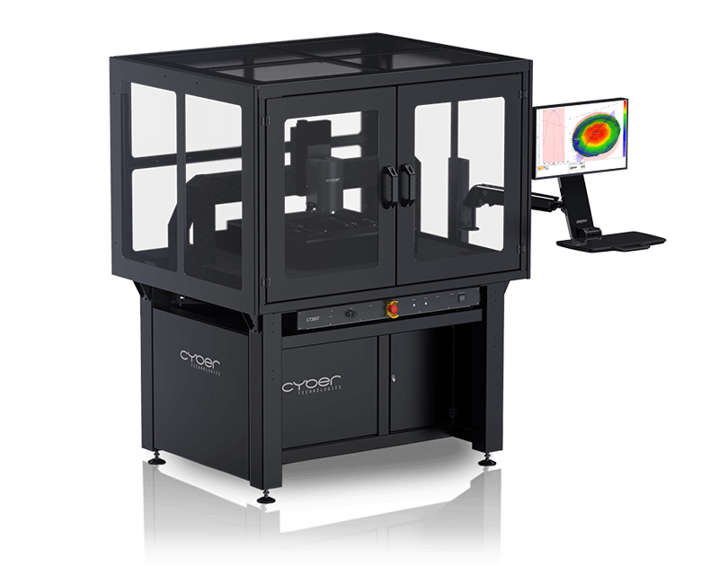
CT350T
Double Sided Metrology System for Production & Laboratory
Modes
Manual / Automated
Scanning Area
329 x 329 mm²
Measurement
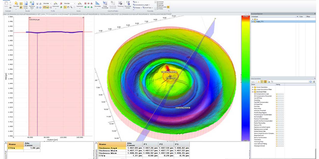
Absolut Thickness (TTV, LTV), Flatness (Bow, Warpage), Heights, Coplanarity (Bumps, Plugs), Position measurement of features of top to bottom surface and many more
Double-Sided Metrology
The CT350T is a cutting-edge, non-contact surface measurement system designed to precisely measure top and bottom surfaces, absolute thickness, and thickness variations simultaneously, ensuring high accuracy across all material types.
Made to Measure
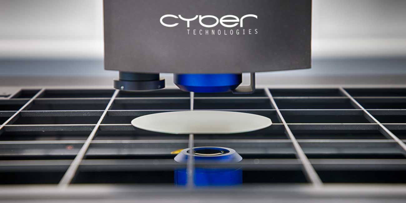
Measure absolute thickness, thickness variations (TTV, LTV), and top and bottom surface in a single run. With dual-sided chromatic confocal sensors, the CT350T achieves sub-micron accuracy. For high-speed applications, line sensors are available, measuring up to 1 million data points per second.
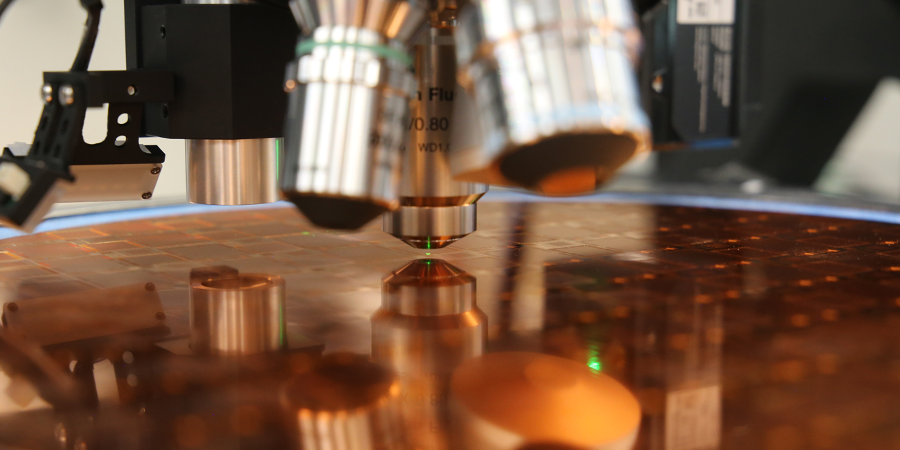
The top axis can be enhanced with additional sensors, making it ideal for various production and R&D applications. Select from five advanced optical sensor technologies, offering ultra-high resolution of up to 0.1 nanometer or high-speed capable of measuring up to 1 million single points per second.
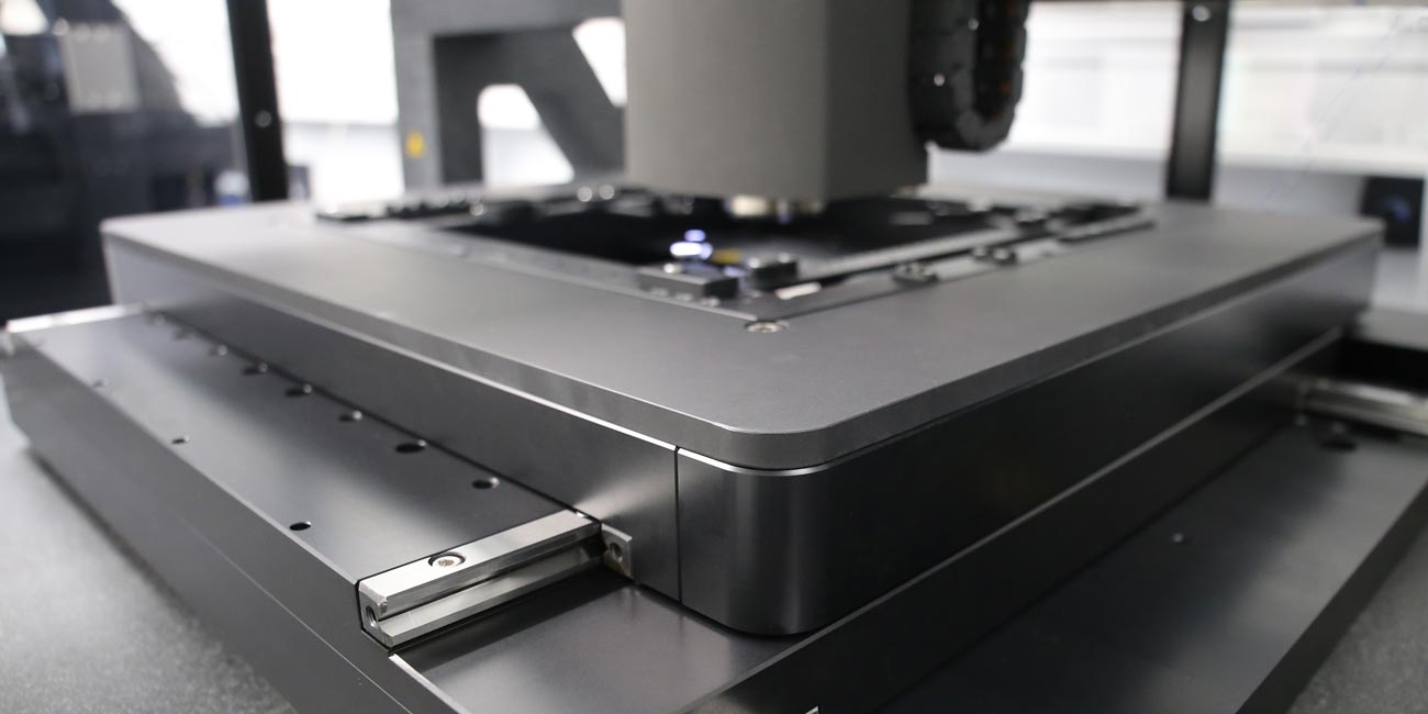
Precise lateral movement on a measurement area of up to 325 x 325 mm². 50 nm encoder ensure pinpoint accuracy for every measurement. Enabling precise positioning and detailed lateral measurements of features. Optionally extend the stage with an interface for your specific samples.
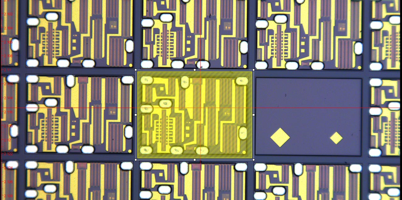
Focus on what matters. The system features a built-in camera with multiple magnification options, allowing you to easily navigate on your samples or choose the sensor’s scanning area in live view. Additionally, the camera enables quick and automated fiducial alignment.
Available Sensors
Flexible high-speed measurements on almost any material with a z-resolution down to 3 nm.
Thickness measurement with a resolution down to 1 nm.
Measure step heights or features with a z-resolution down to 1 nm.
With a z-resolution of down to 0.1 nm for smooth surfaces or smallest (step) heights.
Fast and high-accurate thin film measurement down to 10 nm.
For precise and fast position and lateral measurements with up to 235 MP.
Interested in a configuration of the CT 350T?
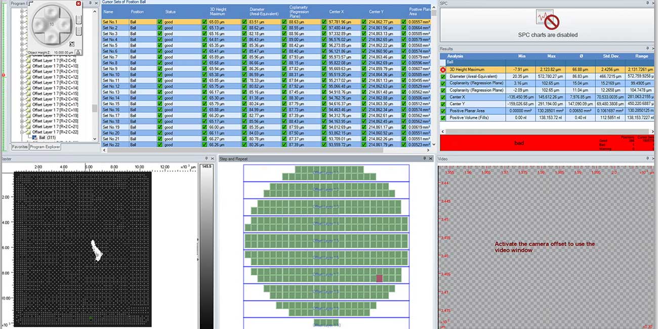
Powerful Analysis
& Automation for Production
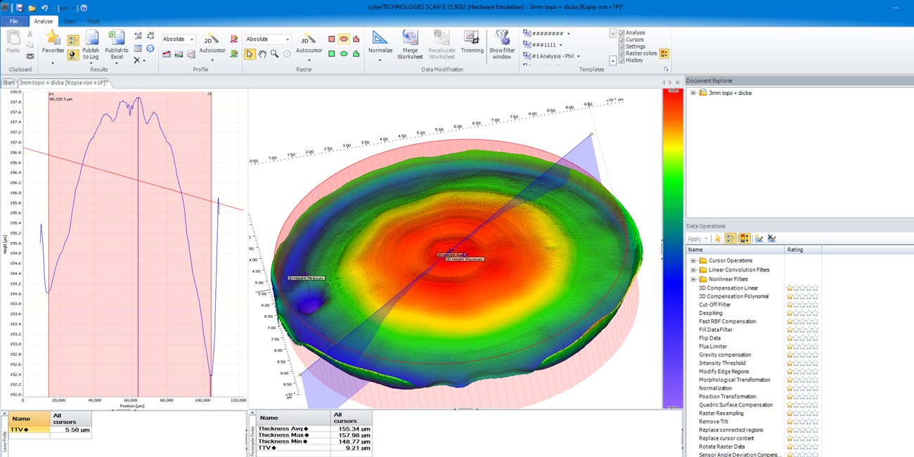
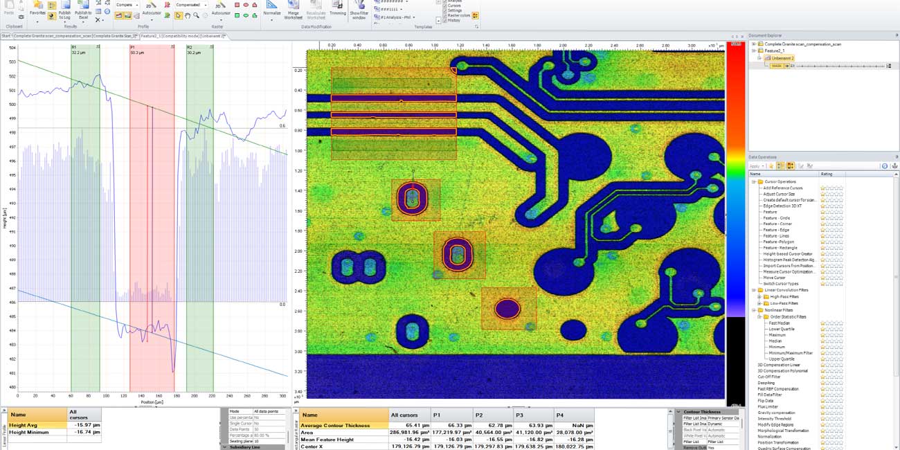
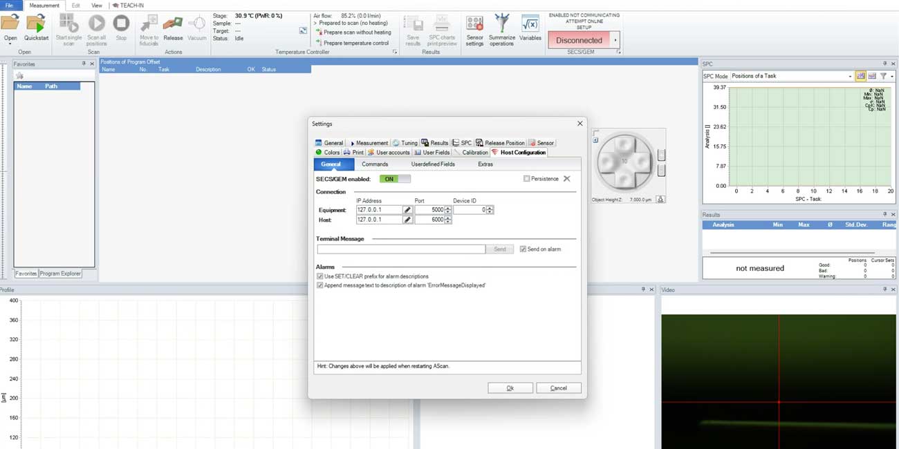
Options
The modular design of the CT-series allows for seamless expansion with a variety of upgrade options. Here’s a quick glimpse of what you can add to enhance your system’s capabilities.
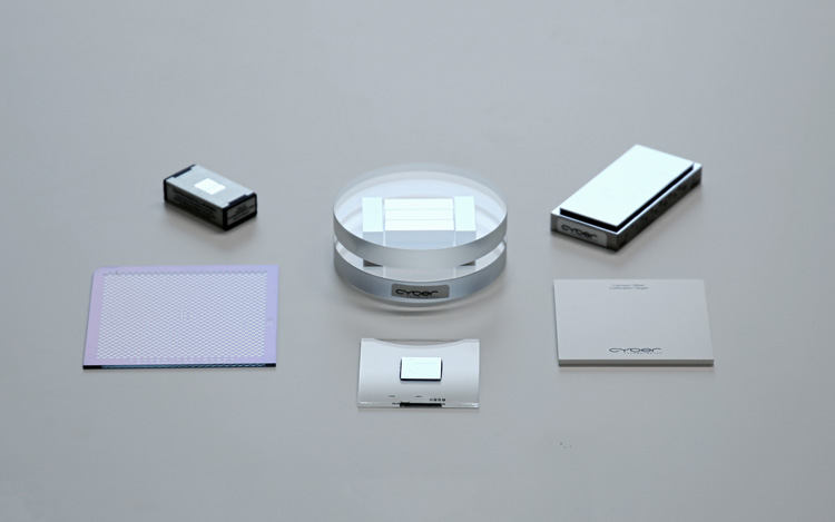
Calibration Targets
Calibrate and certify the system anytime with ease. A wide selection of calibration targets and built-in automated procedures make the process fast and easy.
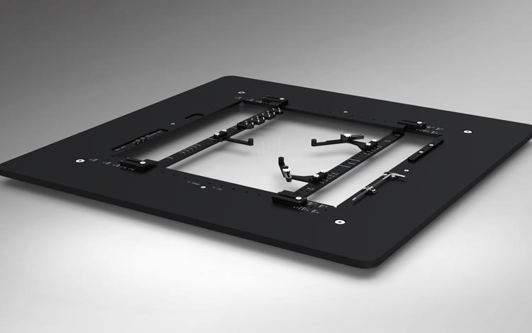
Flexible Interfaces
To ensure secure sample fixation, the system can be equipped for seamless operation and features a fully customizable design for wafers from 4” to 12” or to meet your specific sample requirements.
Configuration Example

CT 350T for Wafer
The CT 350T for Wafer features double-sided chromatic confocal sensors and an interface designed to easily adjust between 4 to 12-inch wafers. It enables simultaneous measurement of absolute thickness (TTV, LTV), warp and bow, all in a single operation. With predefined calibration targets, the system can automatically perform calibration whenever needed.
General
cyberTECHNOLOGIES GmbH
Georg-Kollmannsberger-Straße 3
85386 Eching-Dietersheim
Germany