
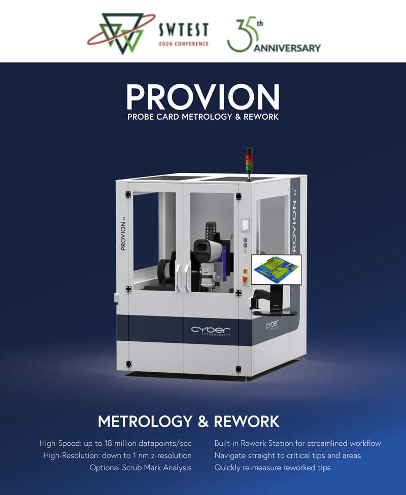
Meet cyberTECHNOLOGIES at SWTest 2026
The event is one of the key technical forums for the semiconductor wafer test industry, bringing together experts in probe technology, wafer-level test, test equipment, materials, and process development.
At Booth 112, we will demonstrate how high-resolution optical metrology can support probe card quality control, maintenance, documentation, and rework.
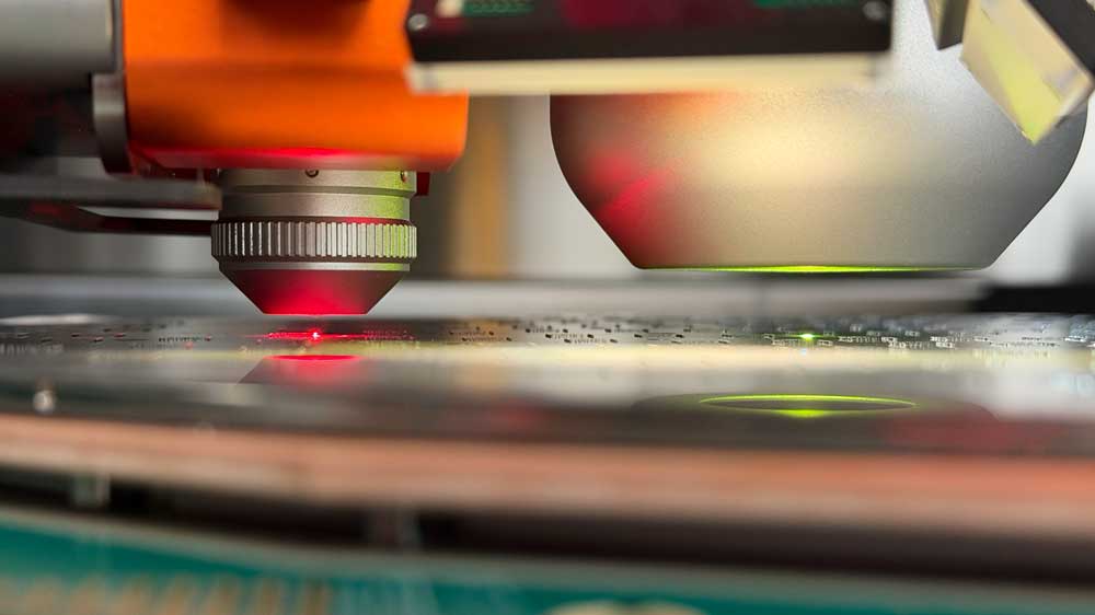
Probe cards are critical interfaces in wafer-level testing, where mechanical contact quality directly influences electrical contact resistance, test repeatability, yield stability, and long-term test reliability.
During operation, probe tips are exposed to repeated mechanical contact, overdrive, scrub motion, contamination, and wear. These effects can lead to changes in probe tip geometry, height distribution, alignment, and scrub mark behavior. Objective measurement data is therefore essential to detect deviations early, document probe card condition, and support data-driven maintenance strategies. Probe tip shape and scrub mark characteristics are known to provide important feedback for evaluating and improving test performance.
With cyberTECHNOLOGIES solutions, users can precisely measure and analyze:
- Probe tip height and coplanarity
- Tip wear, shape, and contact areas
- Bent, shifted, damaged, or missing probes
- Probe alignment and positional deviations
- Surfaces, substrates, and contact structures
- Scrub marks and scrub mark distribution
- Objective measurement data for process control and documentation
- Measurement results to support rework decisions
- Optional probe card rework directly in the same system
By combining high-resolution metrology with integrated rework capabilities, cyberTECHNOLOGIES systems help users evaluate probe card condition with quantitative data instead of visual inspection alone. This enables more consistent maintenance decisions, improved traceability, and better control of probe cards.